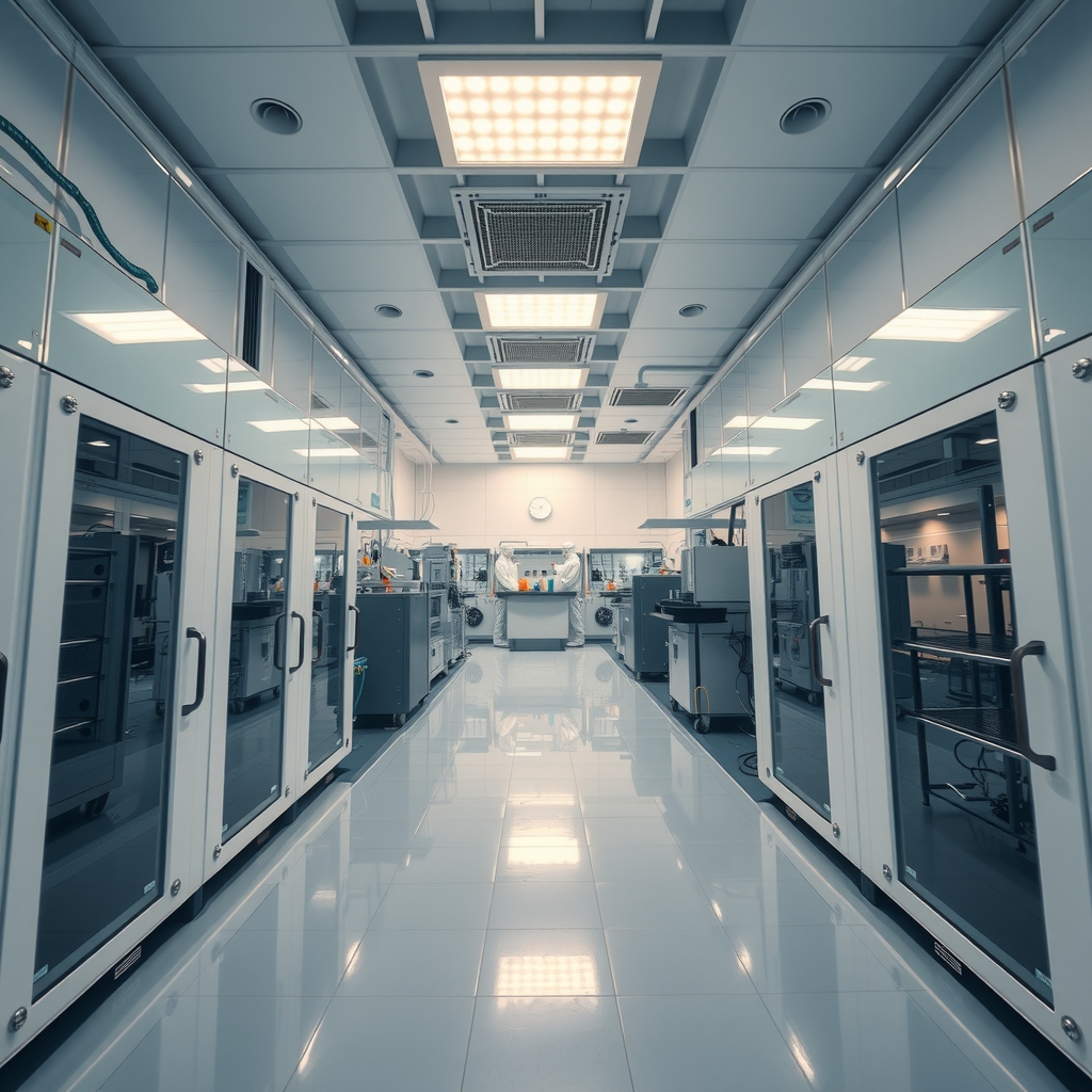

Applied Materials Inc. has officially inaugurated its Equipment and Process Innovation and Commercialization (EPIC) Center, a $5 billion research facility located in Silicon Valley. Designed to serve as a collaborative hub for the semiconductor industry, the center aims to address the growing compute demands driven by the rapid expansion of artificial intelligence infrastructure.
The facility spans over 600,000 square feet and includes nearly four acres of dedicated cleanroom space. By centralizing research and development, Applied Materials intends to foster a collaborative environment where industry leaders can work in parallel on critical manufacturing technologies. According to the company, this initiative is expected to reduce innovation cycles by at least 30%, a vital improvement for an industry currently struggling to keep pace with the demanding development schedules of next-generation AI models.
The EPIC Center brings together a consortium of major industry stakeholders, including Intel Corp., Taiwan Semiconductor Manufacturing Co., Samsung Electronics, Micron Technology, and SK hynix. Additionally, the facility incorporates expertise from innovation partners such as Broadcom and Advantest, alongside academic contributions from institutions including Stanford University and the University of California systems. This collective approach is intended to streamline the co-optimization of complex technologies, such as advanced packaging, 3D architectures, and hybrid bonding.
Applied Materials CEO Gary Dickerson emphasized that the current R&D timeline, which can span up to a decade for new chip technologies, is no longer sustainable in the era of AI. The center is designed to allow engineers to optimize materials and processes before they reach mass production, ensuring that new technologies arrive at fabrication facilities ready for high-yield, high-performance manufacturing. By innovating across materials, process technology, and equipment simultaneously, the company aims to improve energy-efficient computing, which is essential for scaling future AI workloads.
While specific research projects remain undisclosed, the company suggests that the breakthroughs developed at the EPIC Center will have broad implications for consumer electronics, industrial production, and healthcare. As the industry looks toward a future of increasingly complex architectures—with some leaders projecting over a trillion transistors per package by 2030—the collaborative framework established at the EPIC Center is positioned to be a cornerstone of semiconductor advancement, helping to bridge the gap between theoretical research and commercial scalability.